Smart Optics Systems programme (Funding: STW Perspectief)
Image Manipulation for Wafer Plane Conformity in Optical Lithography Systems
| Applicants: |
Prof. Rob Munnig Schmidt (TU Delft, project leader) Prof. Michel Verhaegen (TU Delft) Prof. Maarten Steinbuch (Eindhoven Univ. of Technology) Dr. Nick Rosielle (Eindhoven Univ. of Technology) |
| Partners: | Hans Vermeulen (ASML) Theo Cadee (ASML) Chris Valentin (ASML) Huub Janssen (JPE) |
| Researchers: |
Johan Vogel (TU Delft) Ruxandra Mustata (TU Delft) Geert-Jan Naaijkens (Eindhoven Univ. of Technology) |
|
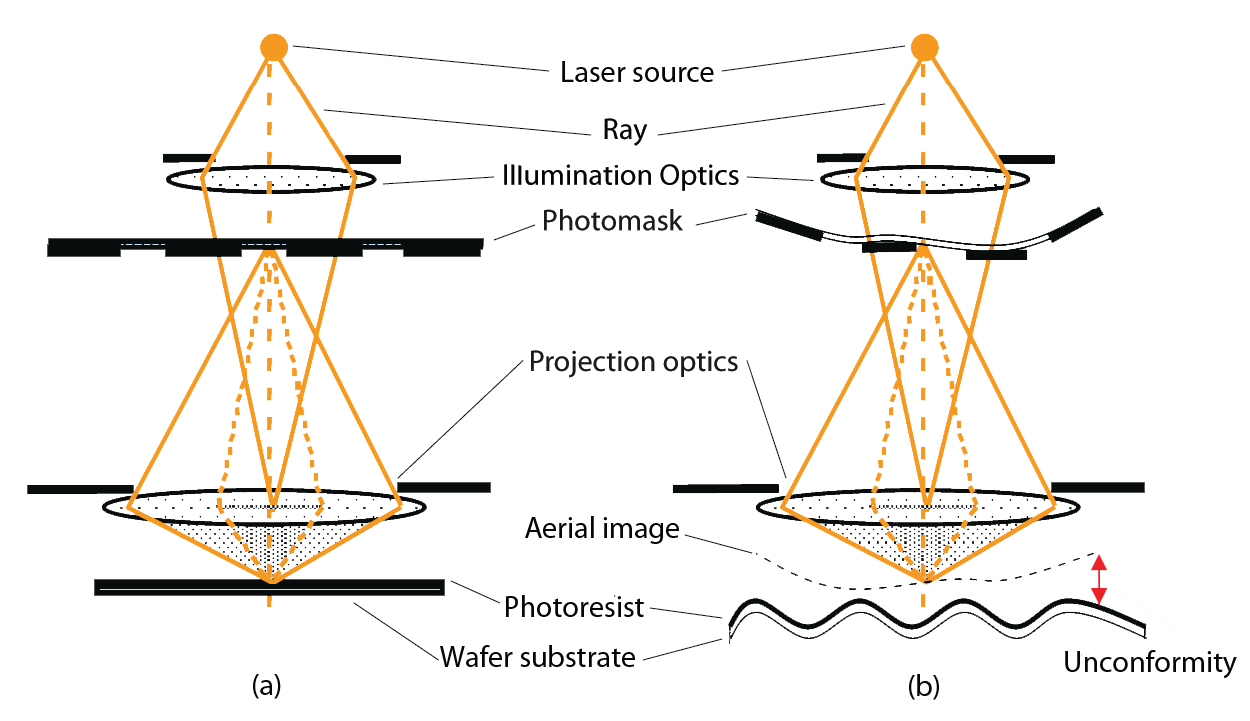
A schematic overview of lithography projection systems, with (a) the ideal projection configuration and (b) the situation with optical path distortions such as photomask and wafer deformation.
|
|
| Project outline: |
The goal of this research is to come to an integral mechatronic design methodology which is generally applicable to opto-mechatronic systems but specifically supports the development of key technologies that increase resolution in high speed imaging systems. The project objective is motivated by the fact that the semiconductor industry is constantly trying to reduce the minimum size, also known as Critical Dimensions (CD), of features that are used to fabricate Integrated Circuits (ICs). A reduction in feature size will result in higher information density and speed as well as reduced power consumption and cost of the IC. These effects improve performance of consumer electronics such as laptops, cellular phones and MP3 players which subsequently lead to increased mobility and economic productivity of society. In the production process of ICs, photolithography is seen as the crucial and limiting step in realizing smaller feature size. In order to facilitate the decrease in CD and improve cost effectiveness of the production process, lithography equipment manufacturers are continuously developing imaging machines with ever increasing resolution and wafer throughput. Up to now, these specifications are achieved by increasing the numerical aperture of the lens and using laser sources with lower wavelengths. Furthermore, the mechatronic system architecture around the lens is optimized to reduce optical aberrations. Considering the ITRS roadmap for lithography, it is clear that ever stringent demands with respect to overlay and CD control are pushing lithography equipment manufacturers to their technological limits. In order to improve conformity of the projected mask image - also known as aerial image - with the wafer surface topology, a number of performance limiting factors need to be tackled. Specifically, static optical path distortions due to lens imperfections and wafer unflatness as well as dynamic distortions due to dynamic deformations and hysteresis of optical path components must be reduced. However, overcoming these effects is becoming increasingly difficult due to the limitations of lens and wafer polishing techniques, use of friction-based (optical) component interfaces and higher component acceleration levels inside lithography equipment to achieve the desired wafer throughput. The push into these extreme machine operating regimes has made it evident that the conventionally applied mechatronic design concepts and technologies have difficulties in tackling the above described problems. In order to be able to develop next generation lithography systems, the current mechatronic approach for imaging systems needs to be enriched with novel opto-mechatronic design rules using Adaptive Optics (AO). Considering its correction potential, the required bandwidth and its proven track record in astronomy [5], AO is seen as the key technology to reduce rapidly changing optical path distortions inside lithography systems whilst keeping complexity and cost to a minimum. To research novel opto-mechatonic design methodologies and investigate the applicability of AO inside high speed lithography systems, the project will utilize a multi-disciplinary approach to simultaneously and iteratively tackle a number of research challenges. Firstly, the use of opto-thermo-mechanical models for adaptive optic actuator and controller design is researched. Specifically, the trade-off between model accuracy and complexity will be investigated. Secondly, the research will focus on the development of an adaptive optic actuation concept for lithography systems at photomask level. Moreover, emphasis is placed on the identification of the actuator number and location that enables an optimized system performance. During this study, additional challenges such as energy dissipation, cost at a minimum of complexity will require dedicated attention. Thirdly, research is required on efficient algorithms to facilitate the multivariable control of, as well as real-time multivariable system and disturbance identification techniques for, high bandwidth AO systems inside lithography equipment. Finally, a metrology system through high speed real-time surface measurement must be developed. It is expected that the above approach will lead to a unique trend change in opto-mechatronic system design methodology and novel technologies for high end optical equipment to meet future requirements of nanometer (nm) level overlay and sub-50 nanometer focus deviations. |